Packaged ICs vs Wafer Level Packaging
MAT anticipates that, in the future, memory chips will be assembled to flexible circuits, either as single or stacked die, without being pre-encapsulated in molding compound (ie. Wafer Level Packaged or Bare Die). This would eliminate a considerable number of “backend” manufacturing steps and their associated costs. The fine lines and spaces obtainable using flexible circuits may even eliminate the need for pre-mounting chips to glass or PCB interposers or processing for pad fanout. Since these WLP or bare die chips will require a protective enclosure, MAT has developed integral heat spreaders that reduce the module thickness to only 2.2mm!
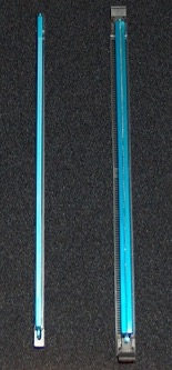
The photograph below illustrates the >40% reduction in cross-section thickness of the assembled WLP flex module on the left with MAT’s standard RDIMM module on the right. The WLP flex module still mates with standard RDIMM sockets, but would benefit from a new socket design that is likewise substantially reduced in cross-section thickness to reduce obstruction of the air flow across the surface of the modules.

WLP Package 2.2mm (left), FBGA Package 3.8mm (right)
Collaborate with the Experts
Contact us to discuss licensing opportunities, design collaboration, or technical consulting.
